Scanning Electron Microscopy (SEM) has transformed the way we explore and understand materials at the nanoscale. However, achieving high-quality imaging often depends on effective sample preparation.
Among the important tools in this process is the sputter coater for SEM, a device designed to address the challenges posed by non-conductive and beam-sensitive specimens.
Whether you’re using a gold sputter coater for SEM or other sputter coating equipment, understanding the process and its benefits is essential for any researcher or lab technician.
What is Sputter Coating for SEM?
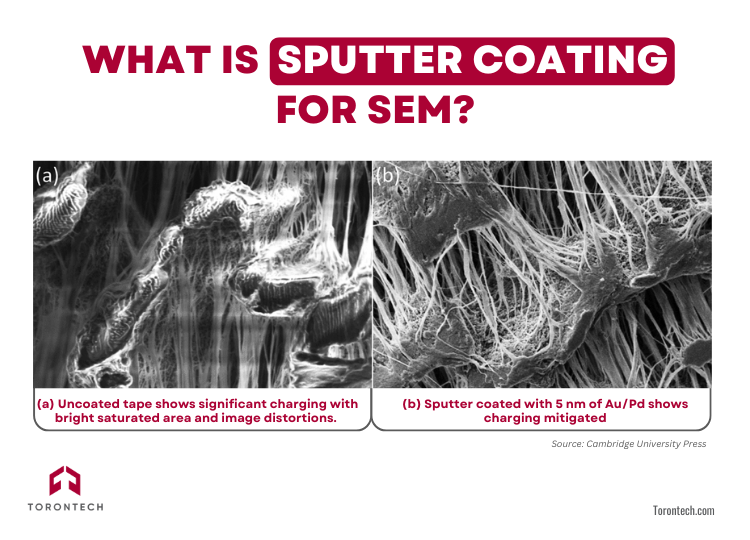
Sputter coating for SEM involves applying a thin, conductive layer to a sample. This layer prevents non-conductive specimens from accumulating charge, which can distort images. It also improves conductivity, enhances clarity, and protects delicate materials during imaging.
The process relies on the sputter coating principle, which happens inside a vacuum chamber. Argon gas is introduced and ionized into plasma. The ions bombard a target material—often gold or another metal—causing atoms to “sputter” and deposit evenly onto the sample. This creates a smooth, conductive layer, making the sample compatible with the SEM environment.
Why Use a Sputter Coater for SEM?

If you’ve faced challenges imaging non-conductive samples, you know how frustrating it can be. Here’s how a sputter coater for SEM solves these problems:
1. Improved Conductivity
Non-conductive samples can build up charge under the electron beam. This charge leads to image distortions, making it hard to get reliable data. A sputter-coated layer dissipates the charge, ensuring accurate results.
2. Sharper Image Quality
The conductive coating reduces noise and increases the signal-to-noise ratio, resulting in clearer, more detailed images. Whether you’re working with a gold sputter coating for SEM or another material, the improvement in image quality is noticeable.
3. Protecting Sensitive Samples
Some samples are sensitive to the SEM’s electron beam. Coating them with a thin conductive layer prevents damage during the imaging process, making the sputter coater for SEM sample preparation invaluable for delicate specimens.
Selecting the Right Coating Material for Optimal Imaging
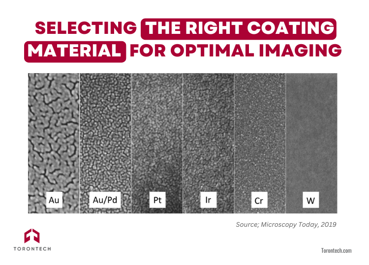
The choice of coating material significantly influences your SEM imaging results. Understanding both the material’s properties and its grain size is essential for achieving the desired outcome. Common materials used in sputter coating systems offer unique advantages tailored to specific imaging needs:
1. Gold (Au)
Widely used due to its high conductivity and secondary electron emission. It’s ideal for general-purpose applications, especially when using a gold sputter coater for SEM. However, its larger grain size (~10–12 nm) limits its effectiveness for magnifications above ~10,000×.
2. Gold/Palladium (Au/Pd) Alloys
These alloys (e.g., 60/40 or 80/20 Au/Pd) produce smaller grains (4–8 nm), making them better suited for higher-resolution imaging at magnifications up to ~25,000×. Their smaller grains enhance image clarity, making them a versatile choice for advanced applications.
3. Platinum (Pt) and Iridium (Ir)
Known for their exceptionally fine grains (Pt: 2–3 nm, Ir: 1–2 nm), these materials are perfect for ultra-high-resolution imaging, even at magnifications up to ~100,000×. They are commonly used in research SEMs where precision is key.
4. Tungsten (W)
Featuring the finest grain size (<1 nm), tungsten is ideal for achieving the highest levels of magnification, up to ~200,000×. Its extreme precision makes it a preferred option for the most detailed imaging needs.
5. Carbon (C)
Unlike metals, carbon is specifically used for X-ray microanalysis. It is applied using specialized methods such as ion-beam sputtering, ensuring a thin, uniform layer for accurate elemental analysis.
When selecting a material, both the application and desired magnification must guide your decision. For general applications, sputter coating gold is a dependable choice.
However, for ultra-high magnifications or specific research needs, materials like platinum, iridium, or tungsten are better suited. Combining the right material properties with the correct grain size ensures optimal results for every imaging challenge.
Applications of Sputter Coating SEM
You might be wondering, “When should I use a sputter coater?” The answer depends on your sample and the type of imaging you need.
- Non-Conductive Samples: Materials like polymers, ceramics, and biological specimens need a conductive layer for distortion-free imaging.
- High-Resolution Imaging: Metals like platinum and iridium are ideal for ultra-high magnification, revealing fine details.
- Beam-Sensitive Materials: A thin, protective coating prevents damage to fragile specimens.
- Elemental Analysis: Coatings like gold enhance secondary electron emission, improving contrast and making analysis easier.
Key Factors for Effective Sputter Coating
Maximizing the performance of your sputter coating machine requires attention to several factors:
- Coating Thickness: A layer between 2–20 nanometers is usually sufficient. Too thick, and you risk obscuring details.
- Vacuum Quality: A high-vacuum system ensures contamination-free deposition and consistent results.
- Deposition Uniformity: Uniform coatings are critical for irregularly shaped samples. Advanced sputter coating systems ensure even coverage.
These considerations help you get the best results from your sputter coater for SEM.
When to Sputter Coat for SEM?
How do you decide if sputter coating is necessary? Non-conductive samples almost always require coating to prevent charging. Even conductive specimens can benefit from sputter coating when higher contrast or better resolution is needed.
While primarily used for SEM, sputter coating is also valuable for Transmission Electron Microscopy (TEM). Materials like iridium and gold enhance contrast, particularly for cellulose nanocrystals and other challenging samples.
Final Thoughts
Using a sputter coater for SEM is a game-changer for anyone working with challenging materials. Whether you’re improving conductivity, protecting sensitive samples, or achieving sharper images, sputter coating ensures better results.
With modern sputter coating systems, you can tailor the process to your specific needs, whether using gold sputter coating for SEM or exploring other materials.
Are you ready to take your SEM imaging to the next level? A well-chosen sputter coating system could make all the difference!
References:
- Heu R, Shahbazmohamadi S, Yorston J, Capeder P. Target Material Selection for Sputter Coating of SEM Samples. Microscopy Today. 2019;27(4):32-36.
- Marina R Mulenos, Bernd Zechmann, Christie M Sayes. Sample Preparation Utilizing Sputter Coating Increases Contrast of Cellulose Nanocrystals In the Transmission Electron Microscope. Microscopy, Volume 68, Issue 6, 3 December 2019, Pages 471–474


