Struggling with poor imaging quality in electron microscopy? Non-conductive samples often lead to frustrating artifacts that obscure your results. It’s a common challenge in material analysis.
You know the stakes are high, accurate imaging can make or break your work. But how do you overcome this barrier? The answer lies in sputter coating, a technique that enhances sample preparation. But what is sputter coating, and why is it critical to achieving precision? Let’s explore.
What is Sputter Coating and Why Do It?
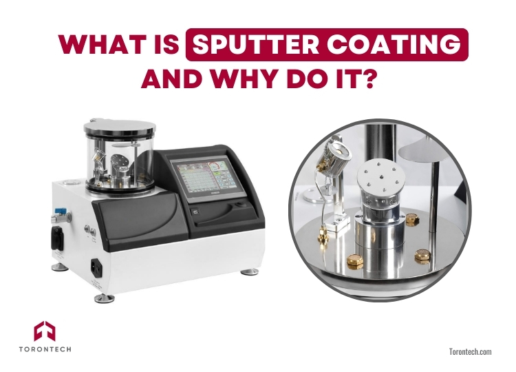
Sputter coating is a transformative technique that creates thin, uniform films on various substrates. Applying conductive materials like gold or platinum eliminates challenges non-conductive samples face during SEM imaging.
These materials offer excellent conductivity, reducing surface charging and enhancing imaging quality (Heu et al., 2019). Thicker coatings, while effective at minimizing charging, may obscure fine structural details.
Sputter coating is also essential in industries like electronics, optics, and materials science, tailored for decorative, functional, and protective purposes (Thornton, 1973). Whether used for sputter-coated components in advanced devices or sputter coating glass for analysis, it ensures unmatched precision and reliability.
Non-conductive samples often build up electrical charges under the electron beam, causing distortions and loss of detail. Sputter coating solves this problem, making samples conductive to improve clarity and reduce artifacts. How does this process actually work? Let’s dive into the mechanics.
How Does Sputter Coating Work?
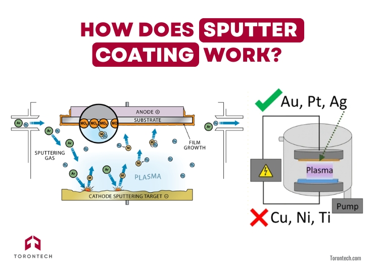
Sputter coating is a sophisticated technique derived from sputtering, a process used to deposit thin films onto surfaces. In this method, an inert gas like argon is introduced into a vacuum chamber and ionized to create plasma.
High-energy ions then bombard a target material, ejecting its atoms, which condense onto the sample to form a uniform thin film. This glow discharge process ensures precise coating, typically 10 to 20 nanometers thick, ideal for enhancing conductivity in SEM imaging and improving surface properties for various applications.
The process accommodates a variety of conductive materials, including gold, silver, and platinum, chosen based on the specific application. These coatings not only eliminate surface charging and enhance imaging clarity but also play a significant role in surface chemistry optimization for advanced techniques like mass spectrometry.
Different metals yield varying sensitivities in molecular interaction, as demonstrated in high-spatial-resolution imaging for laser desorption ionization (Hansen et al., 2019).
From sputter coating glass to applying gold coatings for SEM, this technique ensures that fine details remain visible while providing a stable, conductive surface. Beyond SEM, sputtering is indispensable in microelectronics, optics, and advanced coatings, delivering high-purity films for semiconductor devices, optical lenses, and specialized applications.
The adaptability of sputter coating equipment, including its ability to work with materials like titanium, makes it an essential tool in both research and manufacturing.
Why Do SEM Samples Need Sputter Coating?
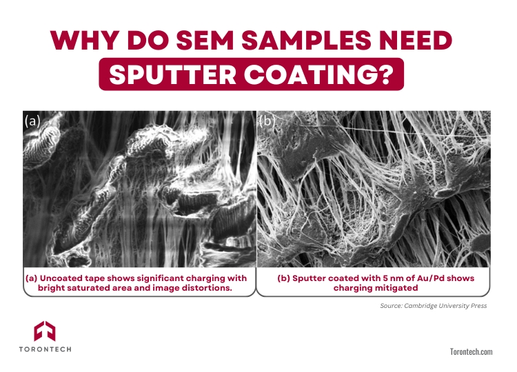
SEM imaging uses a high-energy electron beam, which can cause problems for certain materials. Non-conductive samples often accumulate electrical charges, leading to distortions, while heat-sensitive materials risk damage from the beam’s energy. Sputter coating addresses both issues, making it an essential step in SEM sample preparation.
A thin layer of conductive material, such as gold or platinum, dissipates charges and shields the sample from heat damage. This ensures clear, distortion-free imaging and protects delicate specimens. For researchers working with challenging materials, sputter coating equipment provides the reliability needed for accurate results.
By overcoming these challenges, sputter coating maximizes the performance of SEM technology, making it indispensable for applications in materials science, life sciences, and quality control.
What Industries Use Sputter Coating?
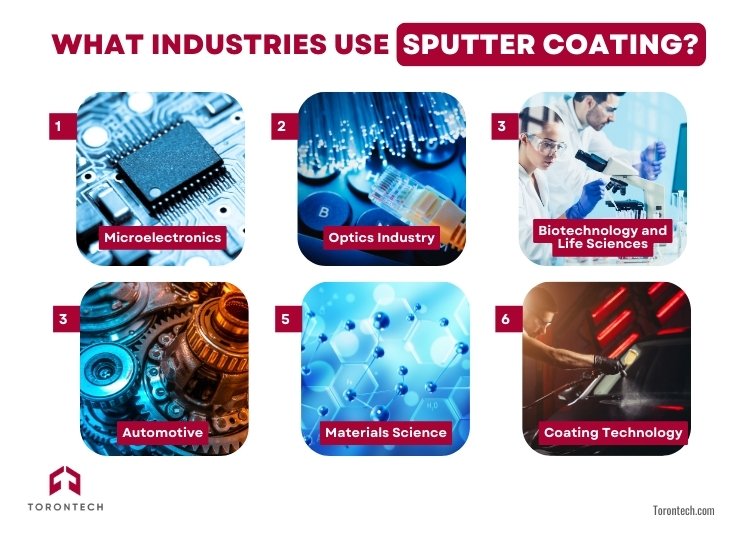
1. Microelectronics
Sputter coating is widely used to deposit thin films on semiconductors, circuit boards, and sensors. These coatings ensure precise conductivity and are critical for creating high-performance electronic components in devices like smartphones, computers, and medical instruments.
2. Optics Industry
Coating materials like gold or titanium onto glass enhances optical properties. This technique improves the performance of lenses, mirrors, and display panels, making it vital for cameras, telescopes, and modern screen technology.
3. Biotechnology and Life Sciences
In SEM imaging, biological samples often require a conductive layer to prevent distortion. Sputter coaters ensure these samples, including cells and tissues, are prepared for high-resolution imaging in fields like cell biology, pathology, and pharmaceutical research.
4. Automotive
Sputter coatings are utilized in automotive applications for producing high-quality reflective coatings and enhancing component durability. The technology also contributes to the production of fuel cells, which are essential for advancing sustainable automotive technologies
5. Materials Science
Sputter coating systems are crucial for studying ceramics, polymers, and composite materials under electron microscopy. Thin, uniform layers make it easier to analyze structural properties without charging artifacts or sample damage.
6. Coating Technology
Sputtering is used to create decorative, functional, or protective coatings. For example, reflective surfaces on consumer products and corrosion-resistant layers on industrial equipment are achieved through precise sputter coating techniques.
What Are the Advantages and Disadvantages of Sputter Coating?
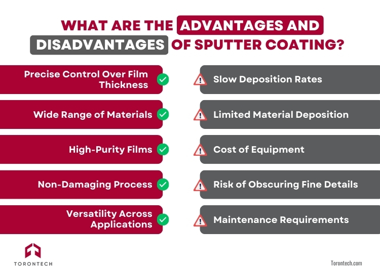
A. Advantages
1. Precise Control Over Film Thickness
Sputter coating systems allow for exact control of layer thickness, typically ranging from 10 to 20 nanometers. This precision ensures consistent results, especially in sensitive applications like SEM imaging or microelectronics.
2. Wide Range of Materials
Materials such as gold, platinum, palladium, and even titanium can be used as target materials, offering versatility for different applications, from enhancing conductivity in SEM samples to improving optical properties.
3. High-Purity Films
The vacuum environment ensures that the deposited films are free from contamination, making the coatings suitable for industries that require high-quality, pure films, such as semiconductor manufacturing.
4. Non-Damaging Process
Unlike some other deposition methods, sputter coating is gentle on delicate and heat-sensitive materials, protecting samples from electron beam damage during SEM analysis.
5. Versatility Across Applications
From sputter coating glass for optics to depositing corrosion-resistant layers, this technique is adaptable to a wide variety of industries, including research and manufacturing.
B. Disadvantages
1. Slow Deposition Rates
Compared to other coating methods, sputtering can be slower, making it less efficient for applications requiring thick layers or high production volumes.
2. Limited Material Deposition
While versatile, sputter coating equipment has limitations when working with certain materials, such as those with very high melting points or specific chemical properties.
3. Cost of Equipment
Sputter coaters and the required vacuum systems can be expensive, making them a significant investment for smaller laboratories or facilities.
4. Risk of Obscuring Fine Details
For SEM imaging, thicker coatings may improve conductivity but can obscure intricate surface details, potentially impacting the accuracy of analysis.
5. Maintenance Requirements
The vacuum chambers and ionization systems need regular maintenance to ensure consistent performance, which can increase operational costs over time.
What is the Difference Between PVD and Sputter Coating?
PVD (Physical Vapor Deposition) refers to techniques that convert solid materials into a gaseous state before depositing them as thin films on substrates. In contrast, sputter coating is a specific PVD method where high-energy ions eject atoms from a solid target, depositing them as a thin, uniform layer on nearby substrates.
While PVD is versatile and suitable for thicker coatings across various industries, sputter coating specializes in ultra-thin, precise films (10-20 nm), making it ideal for SEM sample preparation and enhancing conductivity. PVD is often used for functional and decorative coatings, whereas sputter coating excels in applications requiring precision and uniformity.
Final Thought
Sputter coating is an indispensable technique that bridges the gap between scientific precision and practical application. Whether you’re preparing samples for SEM imaging, enhancing optical performance, or creating thin films for advanced devices, this process delivers unmatched uniformity, conductivity, and reliability
Its adaptability across industries like microelectronics, materials science, biotechnology, and others, underscores its value in modern research and manufacturing.
From addressing challenges with non-conductive and heat-sensitive samples to enabling the creation of high-purity films, sputter coating remains a cornerstone of innovation. As technology advances, its role will only expand, making it an essential tool for achieving consistent, high-quality results in a range of fields.
References:
- Thornton, John A. “Sputter Coating— Its Principles and Potential.” SAE Transactions, vol. 82, 1973, pp. 1787–805. JSTOR.
- Heu R, Shahbazmohamadi S, Yorston J, Capeder P. Target Material Selection for Sputter Coating of SEM Samples. Microscopy Today. 2019;27(4):32-36.
- Hansen, R.L., Dueñas, M.E. & Lee, Y.J. Sputter-Coated Metal Screening for Small Molecule Analysis and High-Spatial Resolution Imaging in Laser Desorption Ionization Mass Spectrometry. J. Am. Soc. Mass Spectrom. 30, 299–308 (2019)
- Heu R, Shahbazmohamadi S, Yorston J, Capeder P. Target Material Selection for Sputter Coating of SEM Samples. Microscopy Today. 2019;27(4):32-36.

